Rok 2026
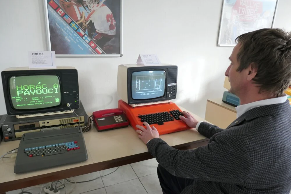
Oprava mikropočítača Maťo.
Typickou poruchou mikropočítača Maťo je, že zdroj nedodáva záporné napätie -5V. Meriame ho voltmetrom - na 4 kolíkoch. Priložíme záporný pól voltmetra na modulátor (GND, zem) a meriame na 4 kolíkoch. Ak nájdeme +12V, +5V, 0 a 0 , tak nám chýba -5V vetva. To je tá najslabšia vetva zdroja, bez tranzistorov a 7805. Príčinou býva zničená dióda D7 - (slabá KA 261) (tesne pri veľkom elektrolytickom kondenzátore C5 - najväčší). Príčinou zničenej diódy D7 je logicky poškodený tantalový kondenzátor C8. A to sa presvedčíme tak, že nahradíme diódu D7 silnejšou, čo doma nájdeme. Po zapnutí zdroja dôjde veľmi rýchlo k vypnutiu tavnej poistky 125 mA. Poistku dočasne nahradíme 500 mA. Zapneme Maťa a kondenzátor C8 nám zhorí. Nahradíme C8 nejakým súdobým ekvivalentom na aspoň 25 V a Maťo naštartuje. Ideálne je premerať C8 či nie je v skrate a vymeniť ho spolu s D7 naraz. Ušetríme si riziko požiaru a jednu poistku. Horenie C8 som už zopakoval nie s jedným Maťom, ale vždy. Preto si to tu zapisujem. Tagy - nefunčná vetva -5V počítača Maťo. Maťo nejde.
Jednoznačne je to konštrukčná chyba Maťa - už druhý Maťo bol takto odídený. Na plošnom spoji okolo transformátora je badať vplyv tepla - vytečený šelak z trafa. Maťo sa asi prehrieval (zdroj tepla - najmä lineárny stabilizovaný zdroj), a tak tepelne zdegradovali kondenzátory.
Schémy a všetko potrebné nájdeme v príručke Maťo.
Občas sa v Maťovi, keď je prepálená poistka - stretol som sa s nehermetickým - prasnutým sieťovým filtrom TL1 - TC241. Vyhodiť a nahradiť priamymi vodičmi (ak nemáme nový filter). Lepšie žiadny ako skrat. Už samotné trafo je dostatočný RLC filter na neharmonické frekvencie - v porovnaní s modernými spínanými činskimi šmejdami - a tie sú všade (nabíjačky, LED žiarovky, Inteligetné zásuvky, všetky standby vecičky).
Vylepšenie videovýstupu Maťa - Maťo štandardne ponúka len VF anténny výstup videa. Vyvedený je na kolík vpravo DIN5 konektora, pri pohľade zvnútra. VF výstup je na kolíku č. 1, 2 je GND. Natíska sa otázka prečo nevyviedli kompozitné VIDEO na kolík č.3. A tak ho vyvedieme. Dosiahneme tým kompatibilitu s monitormi PMD60 a krištálovo čistý obraz. Na CPU doske je videosignál už pripravený na vyvedenie - cca 2 cm vľavo od VF modulátora sú dve väčšia pájkovacie krúžky - zľava GND a VIDEO. Presvedčíme sa že do modulátora vstupuje len +5V, GND a VIDEO signál. VIDEO je predpripravené na vyvedenie na konektor DIN5 - kolík č. 3. Takto nám ostane možnosť pripojiť aj cez anténny vstup TV prijímač, aj monitor PMD60 klasickým káblom ako k PMD-85. Dbáme na odizolovanie prepoja od kondenzátorov v zdroji - použijeme elektrikársku pásku.
Moje aktivity v roku 2024 s PMD-85
V roku 2024 som sa zúčastnil stretnutia zberateľov a prevádzkovateľov historickej výpočtovej techniky v Suchej nad Parnou (marec) a ByteFest v Prahe.
ByteFest 25 - 28. 10. 2024, Praha - Toulcuv dvur

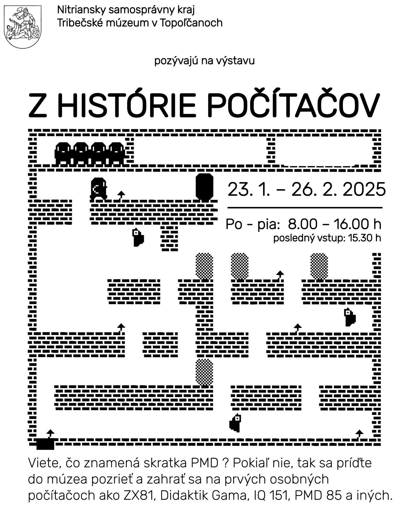
PMD-85 v Topoľčianskom múzeu - rok 2025
Mám naplánované začiatkom roku 2025 výstavu "Zo sveta počítačov' v okresnom múzeu Topoľčany. Miesto konania výstavy nie je náhodné, ale boli vybrané rovnaké priestory, v ktorých sa v rokoch 1986-1996 konali krúžky výpočtovej techniky v ODPM Topoľčany.
Záznam (2 minúty slávy):
Reportáž - TV Markíza Zberateľ Peter má jedinečnú zbierku počítačov
Napísali o výstave v Dnešku
Napísal o výstave Standard.sk
Krátky sprievodný text z múzea:
Počítače v ODPM Topoľčany
V priestoroch múzea, v tejto (zadnej) miestnosti, kde sa nachádzate, sa v rokoch cca 1986 – 1996 konali počítačové krúžky. V budove nesídlilo múzeum, ale ODPM - Okresný dom pionierov a mládeže, neskôr Centrum voľného času Topoľčany. Učebňa zadná, kde sa práve nachádzate viedol zvyčajne pán Ernest Iskra, p. Jozefína Čerešníková. Učebňa obsahovala 4-5 kusov PMD-85-1, jednu tlačiareň D-100, 3-4 kusy SMEP PP-01. Neskôr pribudli stroje ako PP 06, a v 90-rokoch prišlo cca 10 Didaktik Kompakt. Jedného dňa prišla ávia a doviezla vyradené výpočtové stredisko, ktoré sa postupne rozoberalo a slúžilo ako zdroj elektrosúčiastok. Už vtedy – rok 1993 bolo jasné, že je nerentabilné mať sálový počíťač s výkonom 1/3 PC 286. S PMDčkami sa chodilo dokonca na letné sústredenia do Omastinnej. V roku 1994 sa bežne programovalo v BASICu na PMD85, hoci prechod na PC bol nezvratný. Začiatky s PMD-85 boli naozaj o nadšení z novinky – školenia vedúcich prebiehali na obmedzenom počte PMD-85 nonstop (aj v noci) – každý si tú svoju hodinku za PMD85 veľmi rád vyčkal.V prednej učebni, nachádzajúcej sa hneď pri dverách múzea, bola učebňa v spolupráci s HifiKlubom Topoľčany (dnes SSE – Slovenská spoločnosť elektronikov), kde sa nachádzalo cca 10 PMD-85/2 a kde sa viedli krúžky programovania v Karlovi (vedúci Ing. Jozef Boháčik) a v BASIC (Ing. Milan Kopča). Súčasťou učebne bola aj sieť, naraz sa dal nahrať program do všetkých PMDčiek. To zadná učebňa nemala. Do prednej učebne chodili dokonca škôlkari na PMD85 – základy programovania - CIRKUS ŠAŠA TOMÁŠA (p. Oľga Mancová, p. J. Čerešníková). Učebne mali vždy kôpku PMD85 mimo prevádzky (pokazené). Počítače PP01 – za tými zase nikto nechcel pracovať, neboli pre ne žiadne programy, ani hry - eldorádo programátorov v BASICu.
Po vyše 30 rokoch je česť zapnúť v týchto priestoroch PMD85 a zaspomínať na zašlé časy…
Hľadanie si práce v odbore
Taká ožehavá téma. Človek chce niečo nové vyskúšať, naučiť sa, resp. otočiť kormidlo kariéry aj o viac ako 5 stupňov. Ja mám takmer polovicu kariéry v podstate za sebou. Čiže mám 40+ rokov. Skúsil som reagovať neoptimalizovaným CV na prácu, ktorá by som si vedel predstaviť robiť ďaľších 20 rokov. A prišla krásna odpoveď, ktorá medzi riadkami oznámila že nehľadajú 40tnika, pretože 2 roky školení a 18 rokov služby sa im už nevyplatí. Ďaľší dôvod je že môj CV sa nehodí na výkon monotónnej 3smennej práce, kde je mimimum priestoru pre improvizáciu či kreativitu (všetko sa rieši podľa schálených predpisov, je to predsa atómka). Ale to je tak všade, každý šéf hľadá pracanta na konkrétnu prácu, ale nie príliš šikovného, aby ho kariérne nepreskočil. Preto je niekedy vhodnejší pracovitý absolvent.
Vážený pán XYZ,
ďakujeme za Váš životopis, veľmi si vážime, že ste prejavili záujem pracovať práve pre Slovenské elektrárne na pozícii Operátor sekundárneho okruhu.
Po dôkladnom zvážení Vašich skúseností sme sa rozhodli do užšieho výberu vybrať iných uchádzačov ktorých skúsenosti lepšie zodpovedajú naším aktuálnym potrebám.
Keďže nás Váš životopis a pracovné skúsenosti zaujali, budeme radi, ak nám zachováte priazeň aj naďalej a budete sledovať našu stránku WWW, prípadne náš LinkedIn. Tam pravidelne uverejňujeme aktuálne pracovné ponuky, ktoré by Vás mohli zaujať.
PMD-85 colorAce
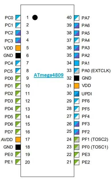
I started play with new Microchip AVR devices: ATMega4809-PF in DIL40 package and AVR128DA28.
ATMega4809-PF is product of post-2016 merge of Atmel with Microchip company.
The ATMega4809-PF is a new (and the only new) single-chip AVR microprocessor in a DIL40 package. Other new processors are SMT versions, e.g., TQFP.
A quick look at the datasheets, which have added a few hundred pages, gives a glimpse of the new product from the megaAVR 0 series family. Among the main novelties, I consider 48 KB flash and 6 KB RAM, while the flash content is mirrored in the address space of 64 KB RAM due to better addressing, not only through LPM instructions. Hence, the exotic 48KB and not 64KB. The RAM size is not a power of two, for example, 8KB.
* I consider the integration of the internal 16/20MHz oscillator a big plus, meaning no external piezo crystal or capacitors are needed. We save outlets and the price of the board.
* Another big plus is doubling the speed of CBI and SBI—setting and resetting the bit of a specific port. This was an early fix for some internal AVR architecture bug; after all, changing one bit in an 8-bit register can't take as long as multiplying 8-bit numbers.
* acceleration of PUSH and ST instructions (writing to stack and writing to RAM)
* Among the main disadvantages, I consider only 33 GPIO ports, of which only 2 are 8-bit PORTA and PORTD. PORTE is 4-bit, PORTC is 6-bit, PORTF is 7-bit, and the Atmega8515 still had up to 4 8-bit ports + 3-bit PORTE. GND has taken its toll, and VDD is on several pins around EMC, AVDD, and a separate UPDI pin. With the addition of the UPDI programming interface, you need to purchase another programmer or make a jtag2updi from an Atmega328 arduino like I did. The only positive is that you connect UPDI via 3 pins; SPI ISP was up to 6 pins. So usable digital GPIOs are 8+8+6+4+7=33 bits. Two pins are the power supply. The 40-35=5 pins of the DIL package cannot be used.
How can we increase, e.g., PORTC to 8-bit? I think it can be done by mapping PC6 and PC7 bits that actually exist via CCL (custom configurable logic) to other ports/pins, for example, PF0=PC6 and PF1=PC7. So we get a full-fledged 8-bit port C. When we have 3 8-bit ports, that's good for us because even the 8080 processor had a 16-bit address and an 8-bit data bus. We'll be fine...
* The advantage of Microchip's new approach is creating a CPU line with scaled FLASH 8,16,32, 48 KB, and 28,32,40,48 pin cases. Even this already gives 16 options + different cases for SMT TQFP, MFR, QFN, and SSOP. This provides realistic dozens of combinations * If you choose an unsuitable CPU, expect 52 weeks of storage. I decided for the ATmega4809-PF, the only one in the DIL40 case. Inside is the same chip as for the TQFP 48 case; only 8 pins are not connected. It's pretty logical and beautiful. Attention—the TQFP 48 case is cheaper than the DIL40. Here, I hesitated whether to go classic (few expensive pins) or SMT (future). * The increased complexity of the ATMega4809 microcomputer is confusing. Golden ATmega. There are so many IO registers, and most of them are memory mapped - MMIO. But there is an effort to clean up. For example, when there are 6 USARTs, each is the same. They differ only in the base address. Each one then has its own 16 registers. * Assembly language programming is no longer for the masses; it's not in the manual, but we'll try.
I created an LED blinker (LED blink or flasher) as a first project to test the new mega4809 processor. Of course, it is connected to PORTE0 through a resistor. I couldn't find a sample program in the assembler anywhere for such a simple thing, so I created it.
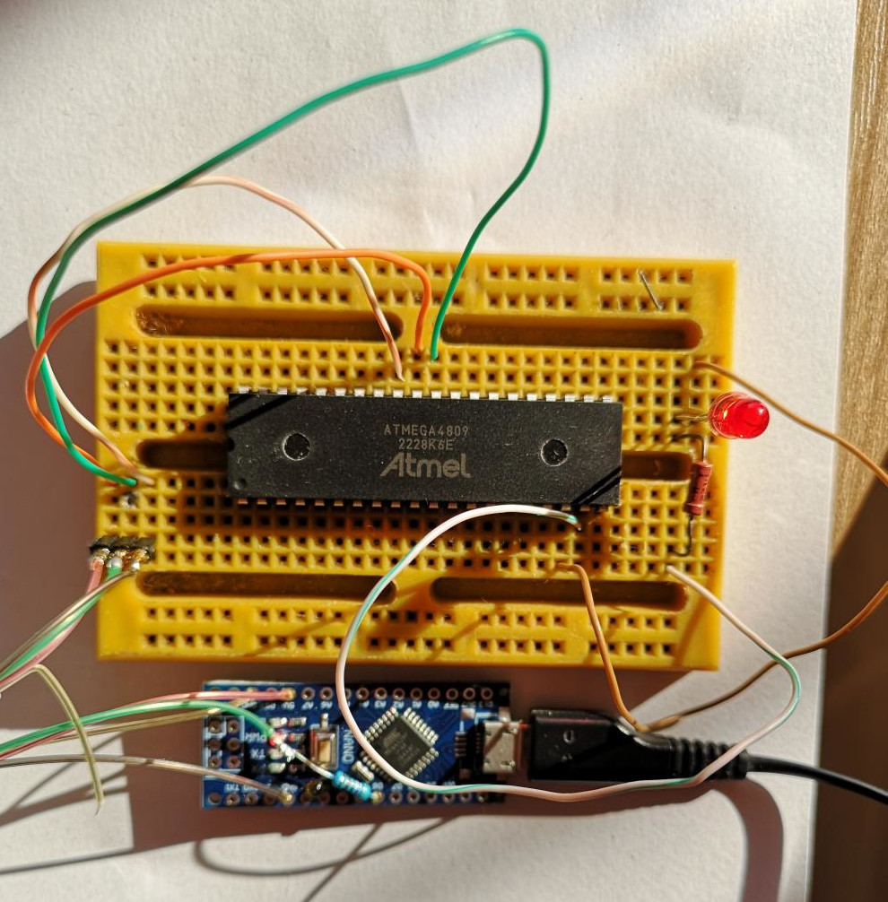
AVRA   Ver. 1.4.2 pmd.asm Fri Apr 12 09:55:28 2024


         	; mega4809 test
         	; BLINK LED DIODE connected to PORTE0 (pin 19 on DIL40 ATMEGA4809-PF)
         	; pure assembly language
         	; (c) wurmi 2024

         	; for program device use command: avrdude -c jtag2updi -p m4809 -P /dev/ttyUSB0 -U flash:w:pmd.hex

          		.device		ATmega4809

          		.def	_zero		=	r10
                .def	_255		=	r22

          		.equ	xDDRE		=	0x0480+0
          		.equ	xPORTE		=	0x0480+0x04

          		.equ	DDRE		=	0x10+0
          		.equ	PORTE		=	0x10+1
          		.equ	PINE		=	0x10+2


         		; CPU is base 0x0030
          		.equ	CPU 	=	0x0030
          		.equ	SPL		=	CPU+0x0D
          		.equ	SPH		=	CPU+0x0D+1

          		.equ	CPU_CCP =	CPU+4

          		.equ	RAMEND	=	0x3FFF

          		.def	XH	= r27
                  .def	XL	= r26
                  .def	YH	= r29
                  .def	YL	= r28
                  .def	ZH	= r31
                  .def	ZL	= r30

                 ; base of CLKCTRL is 0x0060
                  .equ	CLKCTRL= 0x60

                  .equ 	MCLKCTRLB	=	CLKCTRL + 0x01

         		; PORTE0 is LED diode

          		.cseg
C:000000 24aa      		clr		_zero
C:000001 ef6f      		ldi		_255,0xff

C:000002 ef0f      		ldi		r16, low(RAMEND)
C:000003 e31f      		ldi		r17, high(RAMEND)
C:000004 bf0d      		out	   	SPL,r16
C:000005 bf1e      		out		SPH,r17				; set STACK POINTER

C:000006 ed08      		ldi		r16,0xD8			; magic unlock
C:000007 bf04      		out		CPU_CCP, r16
C:000008 92a0 0061 		sts		MCLKCTRLB, _zero	; disable prescaller /6 -> run at full 16/20 MHZ

C:00000a bb60      		out		DDRE, _255			; whole PORTE to output

          main:

C:00000b d004      		rcall	delay
C:00000c 9888      		cbi		PORTE,0			; output 0 to PORTE0; or set whole PORTE to zeroes: out		PORTE, _zero


C:00000d d002      		rcall	delay
C:00000e 9a88      		sbi		PORTE,0			; output 1 to PORTE0;  or set whole PORTE to ones: out		PORTE, _255

C:00000f cffb      		rjmp	main			; forever blinking

          delay:
C:000010 e4e2      		ldi		ZL,66
          de1:
C:000011 d003      		rcall	delay_ffff			; subroutine call
C:000012 95ea      		dec		ZL
C:000013 f7e9      		brne	de1
C:000014 9508      		ret

          delay_ffff:
C:000015 efaf      		ldi		XL,255
          de3:
C:000016 efbf      		ldi		XH,255
          de2:
C:000017 95ba      		dec		XH
C:000018 f7f1      		brne	de2
C:000019 95aa      		dec		XL
C:00001a f7d9      		brne	de3

C:00001b 9508      		ret


Used memory blocks:
   code      :  Start = 0x0000, End = 0x001B, Length = 0x001C (28 words), Overlap=N


Segment usage:
   Code      :        28 words (56 bytes)
   Data      :         0 bytes
   EEPROM    :         0 bytes

Assembly completed with no errors.
PMD85 - in an AVR128DA28
AVR128DA28 je podivný MCU. Je to 8bitové AVR so 128KB FLASH, 16 KB RAM, bežiace na 24 MHz. Čiže poskytuje relatívne vysoký 8bitový procesor s veľa RAM, veľa FLASH. Ak nerátame radu Xmega, tak celkom vysoké parametre. Vie byť zapúzdrený v DIL28 púzdre. Ale - toto púzdro je také núdzové, poskytuje len 22 IO portov. Púzdria sa v 32, 48, 64 napr TQFP, VQFP. TQFP 64 púzdre mám a šokovalo ma malými rozmermi 10x10 mm. Na dĺžke 10 mm je totiž 16 pinov. To bude radosť spájkovať.
Ako prvé čo som spravil bol blikač. OK, bliká. Ďalšie experimenty smerovali k pripojeniu VGA monitora, monochrómne. Tu som si tak experimentoval, obraz som vygeneroval, pekný, ale trochu sa triasol. Skúšal som to fixnúť, a to tak že interný high-freq oscilátor som skúsil tuniť (ladiť),